8
?2004 Semtech Corp.
www.semtech.com
SC338(A)
PRELIMINARY
POWER MANAGEMENT
may not be required. In this case a 0.1礔 ceramic
capacitor will suffice. The input supply to the SC338(A)
should be bypassed with a 0.1礔 ceramic capacitor.
MOSFETs: very low or low threshold N-channel MOSFETs
are required. Selecting FETs rated for V
GS
of 2.7V or 4.5V
will depend upon the available drive voltage (6.9V from
12V in or 4.85V from 5V in), the output voltage and
output current. For the device to work under all
operating conditions, a maximum R
DS(ON)
must be met to
ensure that the output will never go into dropout:
&
=
)
MAX
(
OUT
)
MAX
(
OUT
)
MIN
(
IN
)
MAX
)(
ON
(
DS
I
V
V
R
Note that R
DS(ON)
must be met at all temperatures and at
the minimum V
GS
condition.
Setting The Output Voltage: the adjust pins connect
directly to the inverting input of the error amplifiers, and
the output voltage is set using external resistors (please
refer to the Typical Application Circuit on page 1).
Using output 1 as an example, the output voltage can
be calculated as follows:
?/DIV>
?/DIV>
?/DIV>
?/DIV>
?/DIV>
?/DIV>
+
"
=
2
R
1
R
1
5
.
0
V
OUT
The input bias current for the adjust pin is so low that it
can be safely ignored. To avoid picking up noise, it is
recommended that the total resistance of the feedback
chain be less than 100k&.
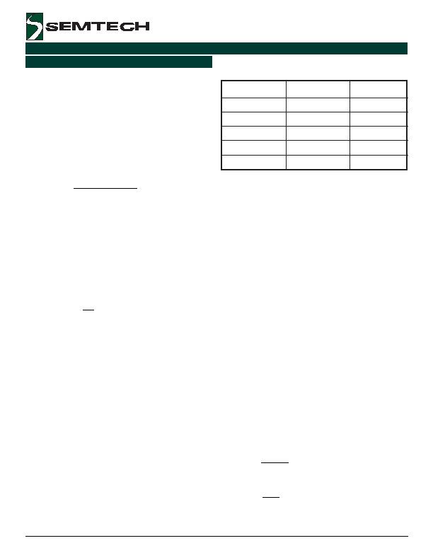
Please see Table 1 on this page for recommended
resistor values for some standard output voltages. All
resistors are 1%, 1/10W.
The maximum output voltage that can be obtained from
each output is determined by the input supply voltage
and the R
DS(ON)
and gate threshold voltage of the
external MOSFET. Assuming that the MOSFET gate
threshold voltage is sufficiently low for the output
voltage chosen and the worst-case drive voltage, V
OUT(MAX)
is given by:
)
MAX
)(
ON
(
DS
)
MAX
(
OUT
)
MIN
(
DRAIN
)
MAX
(
OUT
R
I
V
V
"
=
Applications Infomation (Cont.)
)
V
(
T
U
O
V
k
(
3
R
r
o
1
R
&
&&& &)
k
(
4
R
r
o
2
R
&&&& &)
5
0
.
1
0
.
1
1
0
.
0
1
2
.
1
0
.
4
1
0
.
0
1
5
.
1
0
.
0
2
0
.
0
1
5
.
2
3
.
5
4
3
.
1
1
3
.
3
4
.
3
6
3
.
1
1
Table 1: Recommended Resistor Values For SC338(A)
Design Example
Goal: 1.05V?% @ up to 2.5A from 1.2V?% and 5V?%
Solution 1: no passive droop.
Total window for DC error, ripple and transient is ?2.5mV
Since this device is linear, and assuming that it has been
designed to not ever enter dropout, we do not have ripple
on the output.
The DC error for this output is the sum of:
V
REF
accuracy = ?.5% = ?6.3mV
Feedback chain tolerance = ?% = ?0.5mV
Load regulation = ?.25% = ?.6mV
Set resistors per Table 1 should be 11.0k& (top) and
10.0k& (bottom).
Total DC error = ?.75% = 39.4mV
This leaves ?.25% = 13.1mV for the load transient ESR
spike, therefore:
&
=
=
m
2
.
5
A
5
.
2
mV
1
.
13
R
)
MAX
(
ESR
Bulk capacitance required is given by:
F
dV
t
dI
C
)
MIN
(
BULK
?/DIV>
"
=
Where dI is the maximum load current step, t is the
maximum regulator response time and dV is the
发布紧急采购,3分钟左右您将得到回复。
相关PDF资料
SC402BMLTRT
IC REG DL BCK/LINEAR SYNC 32MLPQ
SC403MLTRT
IC REG DL BCK/LINEAR SYNC 32MLPQ
SC418ULTRT
IC REG DL BUCK/LINEAR 20MLPQ
SC424MLTRT
IC REG DL BUCK/LINEAR 28MLPQ
SC4250LISTRT
IC HOT SWAP CTRLR 8-SOIC
SC427MLTRT
IC REG DL BUCK/LINEAR 32MLPQ
SE95D,112
IC SENSOR TEMP 2.8-5.5V SOT96-1
SE97BTP,547
IC TEMP SENSOR DIMM 8HWSON
相关代理商/技术参数
SC338IMS.TRT
制造商:Semtech Corporation 功能描述:
SC338IMSTR
制造商:SEMTECH 制造商全称:Semtech Corporation 功能描述:Ultra Low Output Voltage Dual Linear FET Controller
SC338IMSTRT
制造商:Semtech Corporation 功能描述:IC CONTROLLER FET DUAL SMD 制造商:Semtech Corporation 功能描述:Controller IC 制造商:Semtech Corporation 功能描述:ULTRA LOW O/P VOLT DL FET CNTL
SC339
制造商:SEMTECH 制造商全称:Semtech Corporation 功能描述:Ultra Low Output Voltage Linear FET Controller
SC3-390RFI
制造商:TT Electronics / Welwyn 功能描述:RESISTOR HIGH POWER 390R 3W 1%
SC339DR2G
功能描述:运算放大器 - 运放 ANA SNGL SUP COMPTRO QUD RoHS:否 制造商:STMicroelectronics 通道数量:4 共模抑制比(最小值):63 dB 输入补偿电压:1 mV 输入偏流(最大值):10 pA 工作电源电压:2.7 V to 5.5 V 安装风格:SMD/SMT 封装 / 箱体:QFN-16 转换速度:0.89 V/us 关闭:No 输出电流:55 mA 最大工作温度:+ 125 C 封装:Reel
SC339EVB
制造商:SEMTECH 制造商全称:Semtech Corporation 功能描述:Ultra Low Output Voltage Linear FET Controller
SC339NG
功能描述:运算放大器 - 运放 ANA SNGL SUP COMPTRO QUD RoHS:否 制造商:STMicroelectronics 通道数量:4 共模抑制比(最小值):63 dB 输入补偿电压:1 mV 输入偏流(最大值):10 pA 工作电源电压:2.7 V to 5.5 V 安装风格:SMD/SMT 封装 / 箱体:QFN-16 转换速度:0.89 V/us 关闭:No 输出电流:55 mA 最大工作温度:+ 125 C 封装:Reel